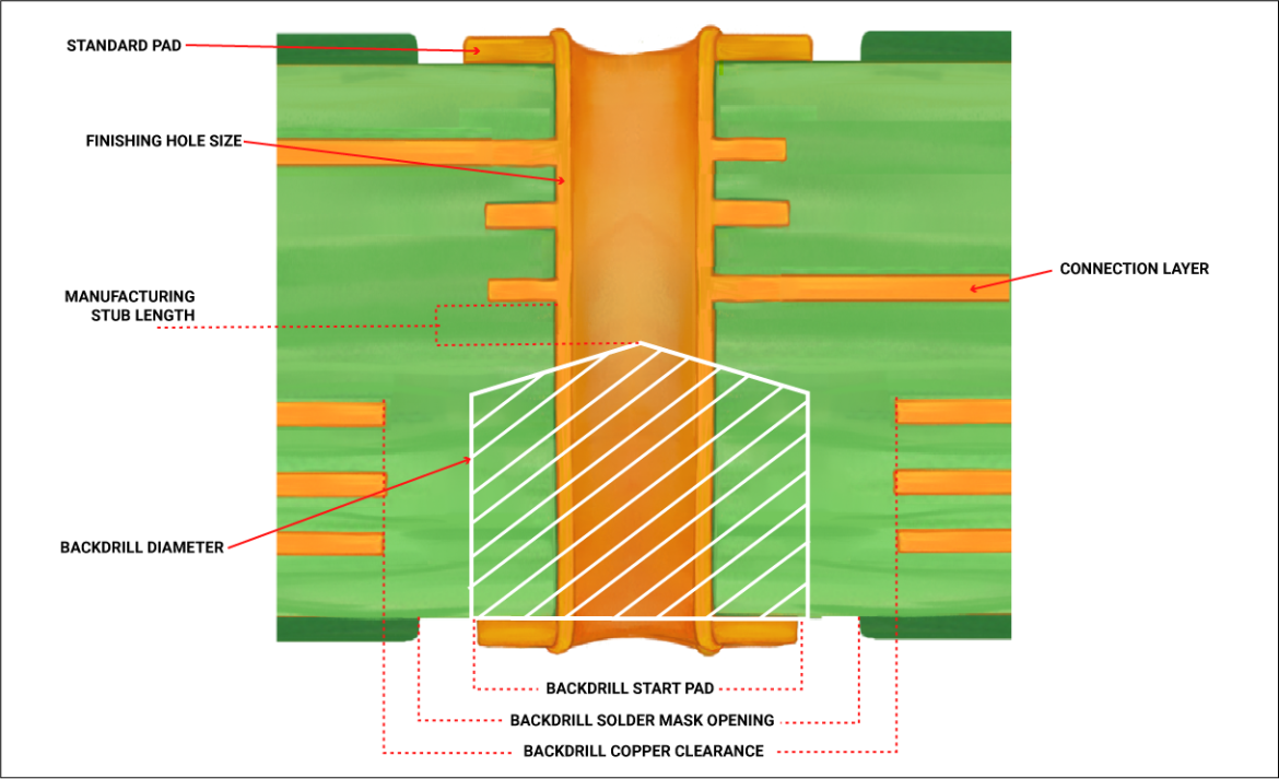
The back drilling process is a crucial technique in the realm of printed circuit board (PCB) manufacturing, primarily employed to enhance signal integrity and performance in high-frequency applications. This article delves into the intricacies of back drilling, exploring its purpose, methodology, benefits, and applications.
What is the Back Drilling Process?
The back drilling process involves the removal of unused segments of plated through-holes (PTHs) in PCBs. These unused sections, often referred to as “stubs,” can cause signal reflections and impair the overall performance of the circuit. By eliminating these stubs, back drilling enhances signal quality and reliability, particularly in high-speed digital and RF circuits.
The Need for Back Drilling
Signal Integrity and High-Frequency Performance
In high-frequency PCB designs, signal integrity is paramount. Stubs in PTHs can act as antennas, reflecting signals back to their source and creating interference. This phenomenon, known as “stub resonance,” can significantly degrade signal quality, leading to data errors and reduced performance. The back drilling process mitigates this issue by removing the unwanted stubs, thereby reducing signal reflections and ensuring cleaner, more reliable signal transmission.
Noise Reduction
Another critical aspect addressed by back drilling is the reduction of electromagnetic interference (EMI) and crosstalk. Stubs can induce noise in adjacent traces, affecting the overall electromagnetic compatibility (EMC) of the PCB. By eliminating these stubs, back drilling helps in maintaining a lower noise floor, essential for the efficient operation of high-speed circuits.
How Back Drilling is Performed
Design Considerations
Before initiating the back drilling process, careful planning and design considerations are imperative. Engineers must identify the vias that require back drilling and determine the exact depth to which the drilling should be performed. This process typically involves advanced CAD software to ensure precision and accuracy.
Drilling Process
- Initial Drilling: The PCB is initially drilled using standard drilling techniques to create the necessary vias and through-holes.
- Layer Identification: The specific layers that require back drilling are identified. This step is critical to avoid damaging the functional sections of the vias.
- Controlled Depth Drilling: Using specialized drilling equipment, the process continues with controlled depth drilling to remove the unwanted stub sections. Precision is key, as the drilling must stop just short of the functional via layers.
- Inspection and Quality Control: Post-drilling, the PCB undergoes thorough inspection to ensure that the back drilling has been executed accurately without damaging the functional parts of the vias. Advanced imaging techniques like X-ray inspection may be employed for this purpose.
Benefits of the Back Drilling Process
Improved Signal Integrity
By eliminating stubs, the back drilling process significantly improves signal integrity. This enhancement is crucial for high-speed and high-frequency applications, where even minor signal distortions can lead to performance issues.
Enhanced Reliability
PCBs with back drilled vias exhibit better overall reliability. The reduction of signal reflections and noise ensures that the circuit operates within its optimal parameters, reducing the likelihood of errors and system failures.
Higher Data Transmission Rates
With improved signal integrity and reduced noise, PCBs can support higher data transmission rates. This is particularly beneficial in applications such as telecommunications, data centers, and high-performance computing, where fast and reliable data transfer is essential.
Applications of Back Drilling
Telecommunications
In telecommunications, where high-speed data transmission is critical, back drilling is widely used to ensure signal clarity and reliability. This is especially important in the infrastructure of modern communication networks, including 5G technology.
Data Centers
Data centers rely on high-performance PCBs to handle massive amounts of data with minimal latency. The back drilling process helps in maintaining the integrity of data signals, ensuring efficient and error-free data handling.
Aerospace and Defense
In aerospace and defense applications, the reliability and performance of electronic systems are of utmost importance. Back drilling contributes to the robustness and efficiency of PCBs used in these critical fields, supporting the stringent demands of military and aerospace operations.
Conclusion
The back drilling process is an indispensable technique in modern PCB manufacturing, addressing the challenges of signal integrity and noise in high-speed applications. By meticulously removing unwanted stubs, back drilling enhances the performance, reliability, and data handling capabilities of PCBs, making it a vital process in various high-tech industries. As technology continues to advance, the importance of back drilling in ensuring optimal PCB functionality will only grow, cementing its role as a cornerstone of sophisticated electronic design and manufacturing.
